
DIFFERENT RIPPLE FOR SAME DESIGN TOPSWITCH 254
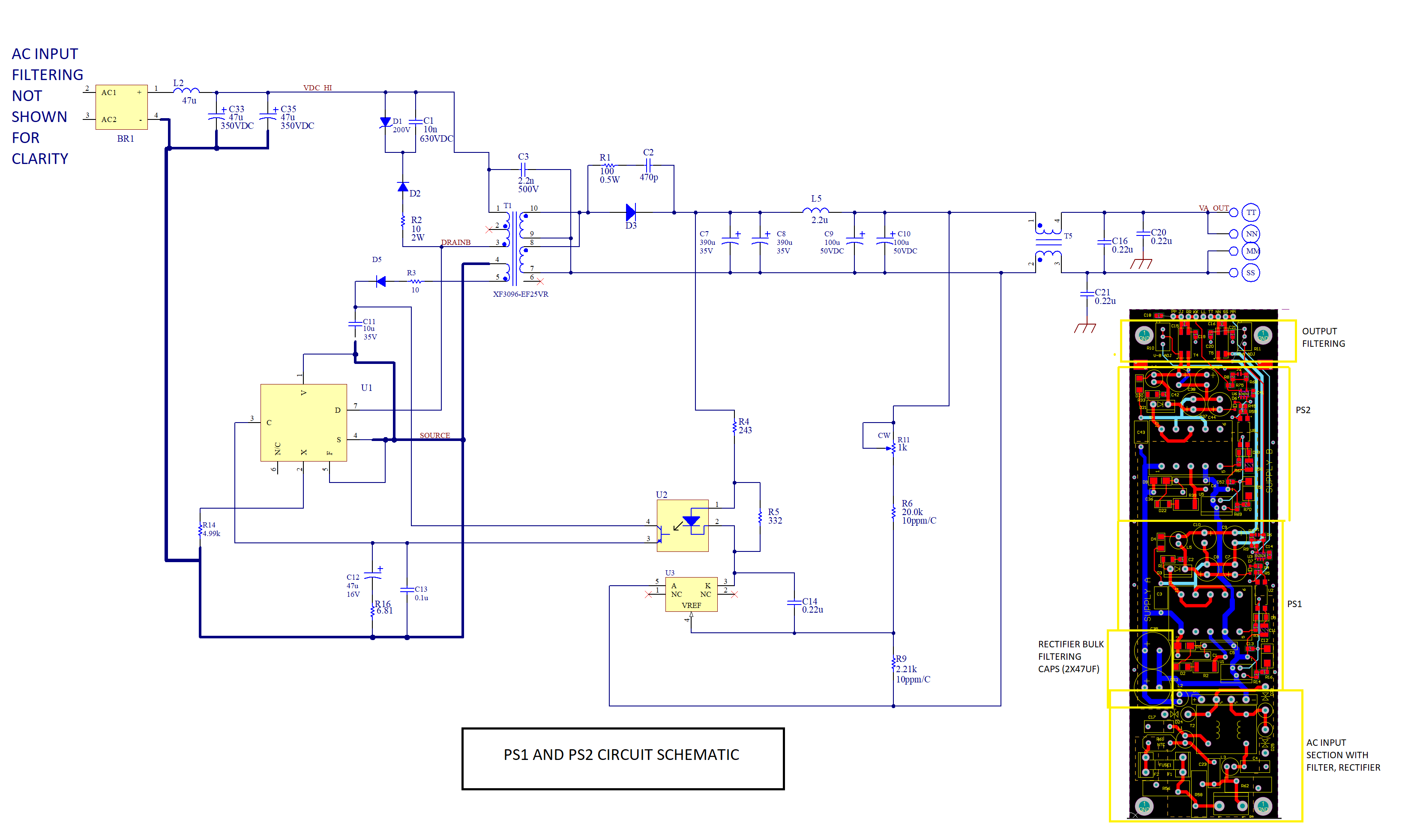
Hi. My application requires I have two 25V supplies in one enclosure, and that they are isolated from the chassis (they will be connected to produce + and - 25V reference to the common connection point). Max output current is 0.5A from each supply which I test into a resistive load. They are the same design, but each has slightly different layout due to the enclosure constraints. My goal is to get 10 mV p-p max ripple under full load. The problem is one supply meets this spec (Power Supply 1, or PS1), but the other is slightly higher (PS2). If they are the same design, and same components why would the loaded ripple be different? I would like to get PS2 ripple under 10 mVpp as well. The ripple in each case appears to be related to the 60Hz line frequency. Note the controller IC is the TOP254.
Some things I tried:
1. Adding bulk rectifier filter capacitance (there already is more than specified by PI Expert)
2. Change feedback component values (vs PI Expert). The values were selected to get the ripple down to 10 mVpp.
3. Bypass the output common mode choke/filtering.
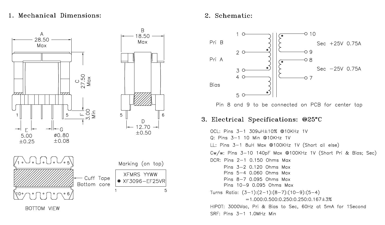
I have attached my schematic plus a sketch of the layout, and PI Expert design as well as the scope captures. The transformer design is also attached.
Appreciate any advice!
Thanks
Files
| Attachment | Size |
|---|---|
| PI expert 25V 0.5A.png | 115.14 KB |
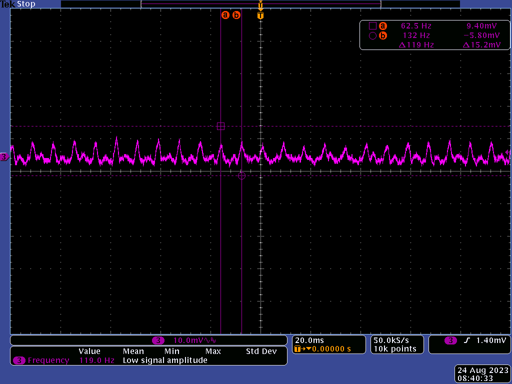
| Ripple of PS1 under full load 0.5 A | 23.41 KB |
| Ripple of PS1 under no load | 18.6 KB |
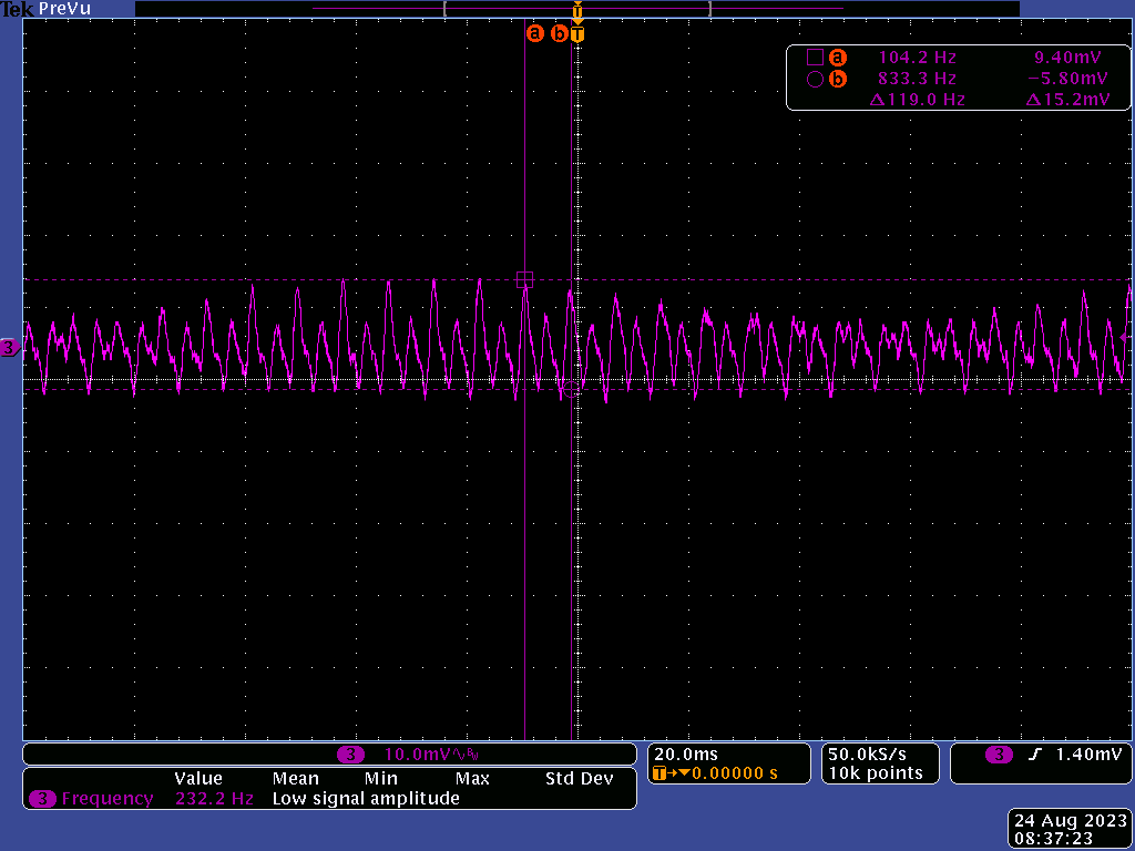
| PS2 0.5 A.png | 27.44 KB |
| PS2 no load.png | 18.82 KB |
| SCHEM WITH LAYOUT.png | 341.55 KB |
| TRANSFORMER.png | 107.26 KB |
Comments
Hi MrScott thanks for your reply. I measured the current through the drain with a current probe and both supplies seem to operating in the same mode - See additional attached scope captures.
I added another thick wire from the bulk filter capacitors to the "Source" of the IC in PS2, just to provide less impedance for the switching curents along the longer trace. This did not make any improvements in PS2 ripple under full load, however PS1 ripple became slightly worse, and now matches PS2's ripple. This suggests layout is a factor, but I am not sure what exactly could be contributing. I will investigate further.
In the meantime can you offer any thoughts on how to reduce ripple under full load in general, perhaps with a applications note, or your experience? These units will be replacing a linear style that has much lower loaded ripple, so there is some motivation to keep it as low as possible (<10 mV pp ideal). The unloaded ripple is around 5 mVpp which would be perfect. In general is it reasonable to expect the loaded ripple to be the same or close to the unloaded ripple?
Thanks again!
| Attachment | Size |
|---|---|
| PS1 Drain Current Full Load (0.5 A).png | 24.11 KB |
| PS2 Drain Current Full Load (0.5 A).png | 24.18 KB |
.png)
.png)
Hi,
Please see AN-43 and AN-47 below for more information on designing with TOPSwitch devices.
https://www.power.com/design-support/application-notes/an-43-topswitch-hx-design-guide
https://www.power.com/design-support/application-notes/an-47-topswitch-jx-application-note
In general, linear power supplies exhibit less ripple compared to switch mode power supplies (i.e. flyback).
The same is generally true for output ripple wherein as the loading condition increases, the output ripple also increases.
Output ripple is also affected by the series resistance (ESR) of the output capacitors used.
You may also try reducing the ESR by using lower ESR capacitors or placing them in parallel connection.
Hi,
Thank you for showing interest in Power Integrations and its products.
Can you confirm that the two power supplies are operating in the same conditions at full load?
You may probe the the TOPSwitch drain voltage/current to confirm the mode of operation.
A quick and dirty test to confirm if the ripple is affected by the layout difference is to switch the components from PS2 to PS1.
The results of this test will give you an idea if the layout differences between the two power supplies is a factor in the ripple produced.